| docs | ||
| ext/TK2000.pretty | ||
| gerbers | ||
| pics | ||
| ROMs | ||
| .gitignore | ||
| fp-lib-table | ||
| LICENSE | ||
| README.md | ||
| TK2000_DiskInterface_REDUX.kicad_pcb | ||
| TK2000_DiskInterface_REDUX.kicad_pro | ||
| TK2000_DiskInterface_REDUX.kicad_sch | ||
| TK2000_DiskInterface_REDUX.pdf | ||
TK2000 Disk Interface REDUX
DISCLAIMER
Any use of this project is under your own responsibility. You will be responsible of checking the correct construction and functionality of your board. By using this project You will agree that I cannot be held responsible if it will destroy any of your devices, damage your computer, burn down your house or whatever.
Sponsorship
![]()
This project is kindly sponsored by PCBWay. PCBWay specializes in manufacturing high-quality PCBs and makes them affordable to hobbyist and professionals alike.
The range of services they offer include PCB prototyping, assembly, instant quotes for your order, a verification process by a team of experts and an easy to use, hassle-free order process.
I'm grateful to PCBWay for the help in evolving and testing this project. You can order the currently released revisions of the board from them, see the link below!
Introduction
The TK2000 had a floppy disk adapter that came in form of a cart, connected directly to the computer, and supported only a single drive connected to it.
Luckily, the adapter was nothing more than a ripoff of the original Apple Disk II interface with some changes to adapt it to the TK2000 bus, so, starting with the recreation by btb as a base, I converted the original interface back to the TK2000, gaining support for a second floppy disk and configurable (via jumpers) I/O and ROM addresses.
This board is meant to be used in the TK2000 bus extender and is part of my project to build a set of cards for the TK2000 computer.
You can build yourself a TK2000 computer using files from this repo and following my build notes.
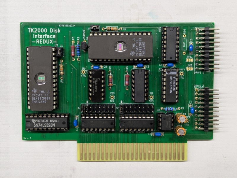
Hardware
The board was designed with KiCad EDA.
Bill of Materials
| Component | Qty | Type / Value | Notes |
|---|---|---|---|
| U1, U2 | 2 | 74LS138 DIP-16 | |
| U3, U8 | 2 | 27C32/64/128/256/512 | Any of these EPROMS will work, as long as the access time is <=100ns |
| U4 | 1 | 74LS259 DIP-16 | |
| U5 | 1 | 74LS05 DIP-14 | |
| U6 | 1 | NE555P or compatible DIP-8 | |
| U7 | 1 | 74LS132 DIP-14 | |
| U9 | 1 | 74LS323 DIP-20 | |
| U10 | 1 | 74L174 DIP-16 | |
| Q1 | 1 | 2N3906 TO-92 | |
| C1, C9 | 2 | 22uF/16V+ 2.5mm electrolytic capacitor | |
| C2 - C8 | 7 | 100nF/25V+ 5.0mm ceramic caps | |
| J5, J6 | 2 | 2x10 2.54mm pin header, right angle | |
| J2, J3 | 2 | 2x8 2.54mm pin header, straight | |
| J1, J4 | 2 | 1x2 2.54mm pin header, straight | |
| R1, R6 | 2 | 10K ohm, 1/4W resistor | |
| R2 | 1 | 560 ohm, 1/4W resistor | |
| R3, R4 | 2 | 2.7K ohm, 1/4W resistor | |
| R5 | 1 | 47K ohm, 1/4W resistor | |
| R9 | 1 | 3K ohm, 1/4W resistor |
The ROMs
The ROMs have the first 8 address lines (A0-A7) connected to the bus, A8 is connected to a pull-down resistor and can be forced high using J1 for U3 and J4 for U8. All the remaining address lines are connected directly to VCC, which means that, following the proper pin alignment, EPROMS from 27C32 to 27C512 can be used.
The original Disk II card used biproms 256 bytes in size, so the dumps needs to be properly concatenated before being used in this card.
If you wish to use 27C512, you can find pre-made files in the ROMs directory (the files used in these are property of Apple).
- U8 houses the content of the P6 ROM
- U3 houses the content of the P5 ROM
Using the premade files will have the 13-sector image loaded when jumpers on J1 and J4 are not installed, and the 16 sector image loaded when the jumpers are installed.
Note that it is not necessary to swap between the 13 and 16 sector state machine (P6/U8, with J4 jumper): You can leave the jumper set for the 16 sector state machine and just swap the boot prom with J1.
Configuring the address
The address for the I/O ports (DEVICE SELECT) can be changed by jumpering J3.
J3: DEVICE SELECT

C C C C C C C C
0 0 0 0 0 0 0 0
8 9 A B C D E F
x x x x x x x x
  ^ default
The address for the ROM (I/O SELECT... confusing, I know) can be set by jumpering J2.
J2: I/O SELECT

C C C C C C C C
1 3 5 7 9 B D F
x x x x x x x x
x x x x x x x x
^ default
The defaults are marked on the board.
Ordering the boards
You can order the board for this project at PCBWay and support me or download the gerbers and have them printed wherever you like!!!